Support material testing and equipment testing
Focus on R & D and manufacturer of plasma cleaning machine for 20 years

How does the plasma surface processor etch silicon nitride and what are its characteristics:
The characteristics of Ni3N4 materials: Ni3N4 is one of the most popular new materials at present. It has the characteristics of low density, high hardness, high elastic modulus, and good thermal stability. It is used in a variety of materials. Silicon nitride can be used in wafer manufacturing instead of silicon oxide. Due to its high hardness, a very thin silicon nitride film can be formed on the surface of the wafer (in silicon wafer manufacturing, the widely used film thickness unit is angstroms). It is about tens of angstroms, which can protect the surface of the wafer and prevent scratches, and its excellent insulation strength and oxidation resistance can also achieve a good barrier effect. Since the fluidity of silicon nitride is not as good as that of oxide, it is difficult to etch. Using plasma surface processor to etch can overcome the difficulty of etching.
Plasma etching is achieved through chemical or physical action, or a combined action of physics and chemistry. During the reaction process, the gas in the reaction chamber is discharged through glow to form a plasma containing active substances such as ions, electrons, and free radicals. These substances will be adsorbed to the surface of the medium due to their diffusion characteristics and chemically interact with the atoms on the surface of the medium. The reaction produces volatiles. At the same time, higher-energy ions will physically bombard and etch the surface of the medium under a certain pressure to remove the redeposited reaction products and polymers. Through the physical and chemical combination of plasma surface processor, the etching of the dielectric layer is completed.
In the wafer manufacturing process, plasma etching is a very important step, and it is also an important link in the microelectronic IC manufacturing process and the micro-nano manufacturing process. Generally, after coating and photolithography development, the plasma surface processor plasma The body undergoes physical sputtering and chemical treatment to remove the unnecessary metal. In this process, the photoresist is a reactive protective film whose purpose is to form the same line shape as the photoresist pattern. The current mainstream dry etching technology is the etching process of the plasma surface processor. Due to its high etching rate and good orientation, it has gradually replaced the traditional wet etching.
Chengfeng Zhizhi has focused on the research and development of plasma cleaning machines for 20 years. If you want to know more product details or have questions about the use of the equipment, please click on Chengfeng Zhizhi online customer service, waiting for your call!
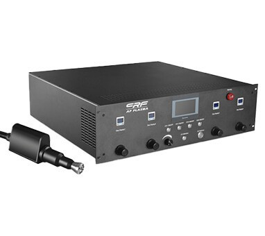
CRF-VPO-4L-S
CRF -APO-IP-XXHD-DXX
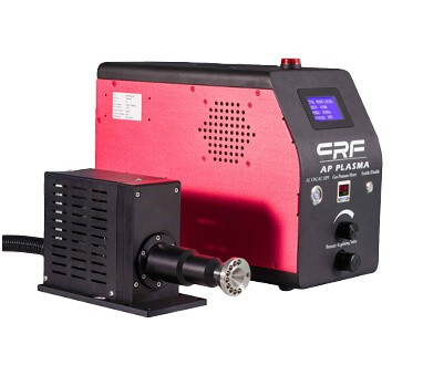
CRF-APO-500W-C
CRF-APO-IP-XXHD-RXX
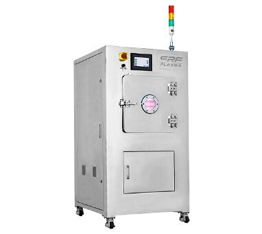
CRF-APO-RP1020-D
CRF-VPO-8L-M
The effect of the oxidizing gas N2 on the conversion reaction under the action of plasma
more >Study on the removal mechanism of micro-nano particles on silicon surface by plasma cleaning process
more >Research progress on the interaction between plasma and catalyst of plasma radio frequency power supply
more >Plasma surface treatment machine is suitable for cleaning plastic industrial materials that are not resistant to high te
more >AFASAGAR plasma spraying machine processing anti-fingerprint, oil stain and anti-reflective functions
more >Chengfeng Zhizhi surface plasma processing equipment for your wafer silicon photoresist removal examples
more >

Official WeChat

Service WeChat

Shenzhen CRF Co., Ltd.
Shenzhen CRF Co., Ltd. Copyright ?2025