Support material testing and equipment testing
Focus on R & D and manufacturer of plasma cleaning machine for 20 years

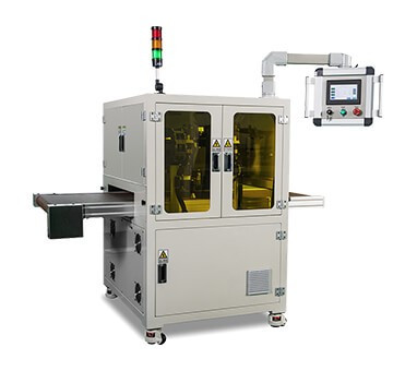
Application of plasma cleaning in BGA packaging process of online plasma cleaning equipment:
In BGA packaging, the substrate or intermediate layer is a very important part. In addition to interconnect wiring, it can also be used for impedance control and inductance/resistance/capacitance integration. Therefore, the substrate is required to have a high glass transition temperature rS (about 175~230°C), high dimensional stability and low moisture absorption, as well as good electrical properties and high reliability. In addition, the metal film, the insulating layer and the substrate medium also have high adhesion.
First, the packaging process of the lead wire of the online plasma cleaning equipment connected to the PBGA

① Use BT resin/glass core board to make extremely thin (12~18μm thick) copper foil, and then drill and through-hole metallization.
Using the traditional PCB plus 3232 process, conduction strips, electrodes, and solder ball-mounted pad arrays are fabricated on both sides of the substrate. Then add the solder mask to make a figure that reveals the electrode and the welding seam. In order to improve production efficiency, usually one substrate contains multiple PBG substrates.
②Packaging process: wafer thinning → wafer cutting → chip bonding → online plasma cleaning equipment plasma cleaning → wire bonding → online plasma cleaning equipment plasma cleaning → molding package → assembling solder balls → reflow soldering → surface marking → Separate→inspect→test hopper packaging chip bonding Adopt silver-filled epoxy adhesive to bond IC chip to BGA packaging process, apply gold wire bonding to realize the connection between chip and substrate, and then use molding encapsulation or Liquid glue potting protects chips, bonding wires and pads.
Specially designed solder balls 62/36/2Sn/Pb/Ag or 63/37/Sn/Pb/Pb with a melting point of 183°C and a diameter of 30mil (0.75mm) are used. Over 230°C. Then, the substrate is centrifuged and cleaned with CFC inorganic cleaning agent to remove residual solder and fiber particles, followed by marking, separation, inspection, testing and packaging.
The above is the packaging process of wire bonding PBGA.
2. FC-CBGA packaging process of online plasma cleaning equipment
① Ceramic substrate The FC-CBGA substrate is a multilayer ceramic substrate, which is difficult to prepare. Due to the high wiring density of the substrate, narrow spacing, many through holes, and high requirements for the substrate to be coplanar. The main process is: first co-fire the multilayer ceramic sheet substrate into a multilayer ceramic metalized substrate at a high temperature, then make a multilayer metal wire on the substrate, and then electroplating. In the CBGA assembly process, the CTE mismatch between the substrate, the chip, and the PCB is the main cause of product failure. In order to improve this situation, in addition to the CCGA structure, other ceramic substrates-HITCE ceramic substrates can also be used.
②Packaging process: preparation of wafer bumps-wafer cutting (chip flip chip and reflow soldering), underfill thermal grease, sealing solder distribution + capping bucket sleeve assembly solder balls-reflow soldering bucket sleeve marking + separate inspection Bucket packaging
3. The packaging process of the lead wire of the online plasma cleaning equipment connected to the TBGA:
① TBGA carrying TBGA is usually made of polyimide material. During manufacturing, the copper sheet is first coated with copper on both sides, then nickel-plated and gold-plated, and then punched and through-hole metalized to form a pattern. In this lead-connected TBGA, the packaged heat sink is the solidification of the package and also the core cavity base of the package. Therefore, before packaging, the carrier tape must be bonded to the heat sink with a pressure-sensitive adhesive.
②Packaging process: wafer thinning → wafer cutting → die bonding → cleaning → wire connection → online plasma cleaning equipment plasma cleaning → liquid sealing → assembly solder ball → reflow soldering → surface marking → separation → inspection → test →Packaging.
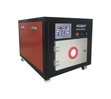
CRF-VPO-4L-S
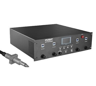
CRF -APO-IP-XXHD-DXX
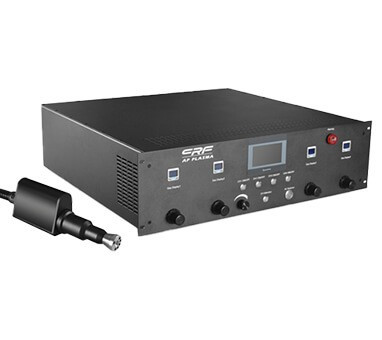
CRF-APO-500W-C
CRF-APO-IP-XXHD-RXX
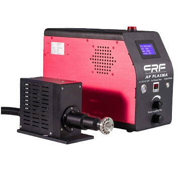
CRF-APO-RP1020-D
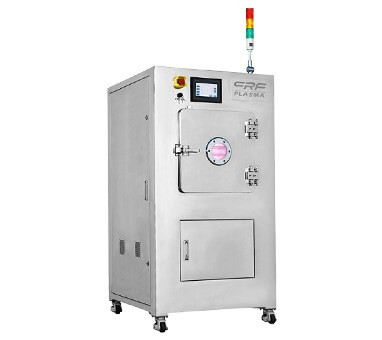
CRF-VPO-8L-M
Research on the modification effect of various high-energy particles of oxygen plasma on the surface of bamboo charcoal
more >The function and process value of the equipment of Chengfeng Zhizhi plasma processor manufacturer to process masks
more >The NGTi-based TIO2 film becomes very dense, smooth and hydrophilic after the etching process of the Ar plasma cleaner
more >The plasma cleaner manufacturer introduces the difference between magnetic binding fusion and inertial binding plasma
more >Plasma PCB cleaning machine PCB faces greater challenges in materials and process technology
more >The improvement of low-temperature plasma surface treatment machine on the surface bonding effect of PTFE materials
more >

Official WeChat

Service WeChat

Shenzhen CRF Co., Ltd.
Shenzhen CRF Co., Ltd. Copyright ?2025